Solbourne Computer

Stacks Image 8

Click here for more info about and larger photographs of the hardware.

Solbourne Computer was an engineering workstation company founded by Doug MacGregor in 1986. MacGregor had designed the microcode for the Motorola 68010 and 68020 microprocessors and then pursued a doctorate in Information Science at Kyoto University. After a presentation in Japan he met a senior executive from Matsushita Corporation who ultimately funded Solbourne (originally called SAE for "Solutions are Everything") in the unlikely location of Longmont, Colorado.

My first job out of college with was with the Technical Workstation Group at Hewlett-Packard in Fort Collins, Colorado. I hired into a group run by Ken Watts. I had no idea how lucky I was to have him for a manager. He was considered one of the best managers in the organization who fought tooth-and-nail for his engineers. At the time Ken's group was designing graphics systems for HP workstations but he knew Doug MacGregor because HP had been one of the first customers of the Motorola 68k line. Doug called on Ken as he started to build a team for his new company and Ken did the unthinkable in those days ...leave HP... along with several engineers. I ended up working for a manager I can barely remember now but disliked intensely at the time. About a year and a half later I got home from the movies with my soon-to-be-wife and found a message from Ken on the answering machine asking if I was done "playing around at HP" and wanted to come down to work with him again. It wasn't a hard decision and I left mother HP for the world of start-ups. Sadly Ken passed away a couple of years later.

Some of the best and some of the worst times I have had as an engineer were at Solbourne. The company was a fantastic place to work in the beginning. We did some amazing engineering and had a great time. The first symmetric multiprocessing SPARC server. Perhaps the first synchronous DRAM (a VRAM with built-in raster-ops). A fast track graphics project I managed that went from initial kickoff to fully functional PCB prototype in 2 weeks. But some major strategic decisions doomed the company to be nothing more than a footnote in the history of computing. The company lived on for many years providing consulting services and solutions based on Oracle Applications and technologies before being acquired by Deloitte.

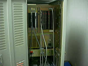
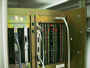
Someday I'd like to document the history of Solbourne. It was an incredible time for everyone involved. At one point I took the pictures on this page of some of the hardware. Sorry for the poor quality. I had only a terrible Apple QuickTake 200 camera that I had gotten as a free promotion from Apple.

Solbourne's first products were based on a cache-coherent multiprocessor bus called K-bus. It supported up to 11 slots using TTL signaling at 20 MHz and was used in three computers: an initial desk side server with 7 slots, a (big) desktop with 5 slots and a rack-mounted server with 11 slots. It had a sustained bandwidth of 108 MB/sec, 32-bit memory addressing and a 64-bit data-bus with ECC.

Solbourne Server from the rear
Solbourne server card cage
Solbourne Series 6E CPU board
My first project was to design and build a K-bus stimulus board which provided a register-mapped interface to a Sun workstation through VME. Software developed by an incredible engineer and wonderful friend, Ty Sell, running on the Sun workstation could generate or record K-bus transactions. The first stimulus board was wire wrapped by a crusty but great ex-IBM tech named Larry Gerber. All TTL logic, it was a sight to behold. I was amazed it worked (I was a junior engineer and I think Larry was amazed too). It was my first experience using PALs for control and the ability to fix logic by reprogramming was forever etched in my design consciousness. We didn't simulate at that time so designs were debugged on the testbench with logic analyzers and oscilloscopes. The stimulus board was used to do initial debug of the 16 MB memory board. Later stimulus boards were built on PCBs. They were used heavily over the years in engineering and manufacturing.
Solbourne 16 MB Memory board

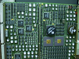
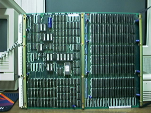
16 MB K-bus memory board

Solbourne 128 MB Memory board

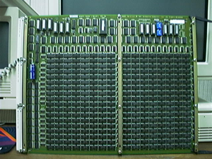
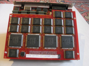
128 MB K-bus memory board

Originally Solbourne was architecting its own CPU (MacGregor, not one to think small, called it KAP for Kick Ass Processor). The marketing VP (I think) was instrumental in convincing the company to adopt Sun's SPARC architecture and it soon became obvious that the software advantage we gained by using SPARC far outweighed any perceived advantage of our own CPU architecture (not that there weren't heated battles about the issue). One of the first clone companies was born. An immediate fallout was that we needed a Sun-compatible frame buffer and since I had some experience with graphics I got roped into designing the "bwtwo" monochrome frame buffer while a more experienced engineer designed the 8-bit dumb color frame buffer. All discrete logic, it supported both 1152x900 and 1600x1280 pixel resolutions (I used ECL logic at 200 MHz for the pixel data). I originally prototyped the circuitry on it's own K-bus board but it ultimately ended up on the system IO board. I made an interesting mistake when moving the schematic from the stand-alone board to the IO board. I had used DIP VRAMs on the stand-alone board but was moving to ZIP parts for the IO board. I forgot to adjust the pinout and it took a bit of head scratching in the lab before I realized what I had done. My manager, Vahid Samee, noticed that the parts had the same signal order (just as they came off the die) so we could mount the ZIP parts in the proto PCB starting part-way up their mounting position and jumper the high pins lower on the PCB. It worked!
Monochrome frame buffer circuitry I designed

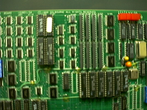
Monochrome circuitry
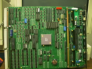
K-bus IO board

K-bus IO board

The early graphics subsystems were memory mapped IO. This was ok for the monochrome frame buffer since it only took about 128k of memory for an 1152x900 pixel display. Unfortunately we found that the 8-bit dumb color frame buffer was agonizingly slow. Since we were now Sun compatible and all the graphics libraries ended up in user code we had to be 100% compatible with Sun's frame buffers. After a short panic we decided to clone Sun's cg3 frame buffer. This board included a raster-op logic engine for each color plane. I got to do it. Each American engineer had a Japanese engineer assigned to work with him by Matsushita. My engineer was incredibly clever and he painstakingly reverse-engineered some of the trickier parts of Sun's design. We called our board the CG30 and it provided much higher performance.
Solbourne CD30 graphics board

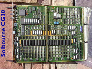
CG30 Semi-intelligent frame buffer

After CG30 the company had started working on it's ill-fated S4000 desktop machine which used Sun's SBus as the IO bus. I was assigned to architect an integrated graphics subsystem for SBus (CG+). We were successful but along with the desktop the project failed. There were a couple of starting conditions that ultimately led us to make wrong decisions regarding the SBus graphics system. One was the PIPRAM graphics VRAM chip that had already been designed but never used. One thing Matsushita was interested in with their investment was designing silicon. The first piece of silicon was a 1280x1024 pixel synchronous VRAM with built-in raster ops. It had a 16-bit data path and operated at 16.67 MHz. Incredibly clever at the time (and quite possible infringed upon by many companies today) it turned out to be way too expensive to compete with commodity parts. The second starting condition for the SBus graphics system was the existence of a 3D graphics software group that had it's origins when the company was founded. They wanted accelerated 3D graphics and since that was sexy and I was young I thought it was the thing to do. My management supported me and we designed a 3D graphics system that supported 8- and 24-bit frame buffers and intelligent DMA from main memory using user-process virtual memory addresses (we directly parsed X11 data structures) with 3 ASICs, 2 AT&T DSP32C processors and the full-custom PIPRAM for the frame buffer and Z-buffer. Unfortunately by this time the rest of the company was focused on supporting the EDA market and 3D graphics were superfluous. Another group in Japan had built a dumb 8-bit color frame buffer and in a stunning repeat of history it was way too slow in the system. In a very exciting and fast-track project we took the graphics engine ASIC, two data path ASICs and 8 PIPRAMs and made the SGA20 accelerated 2D graphics board in just a bit over two weeks including a graphics library that provided compatibility with Sun's 2D applications. We had it ready for the first appearance of the desktop computer at a trade show but MacGregor didn't want to show it (I never forgave him for that). So many people busted their chops on that project. In retrospect I would have forgone both use of PIPRAM and 3D graphics to have done a very inexpensive but accelerated 2D graphics board using commercial VRAMs.
Solbourne CG40 graphics adapter for SBus

CG+ SGA40 Intelligent graphics system

The desktop system had used a home-designed SPARC processor that never met its original goals. The 6 kbyte L1 on-board cache was much smaller than originally envisioned and yields never met the initial 40 MHz goal. The design team wanted to use a faster SPARC processor from Cypress or TI but were overruled by political considerations. The desktop system was a failure even after an upgrade with a 256 kbyte L2 cache and clock rate of 36 MHz. The company never recovered and got out of the computer business completely by 1994.
Solbourne S4000 desktop computer

S4000

Solbourne S3000 desktop computer

S3000